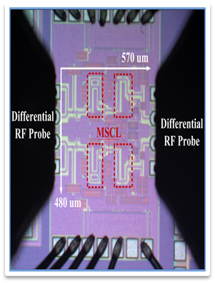
| 40GHz Phase Locked Loop (PLL) |
| |
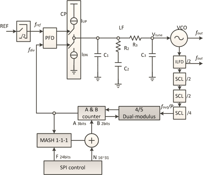 Fig. 1. Block diagram of the designed fractional-N frequency synthesizer.
|
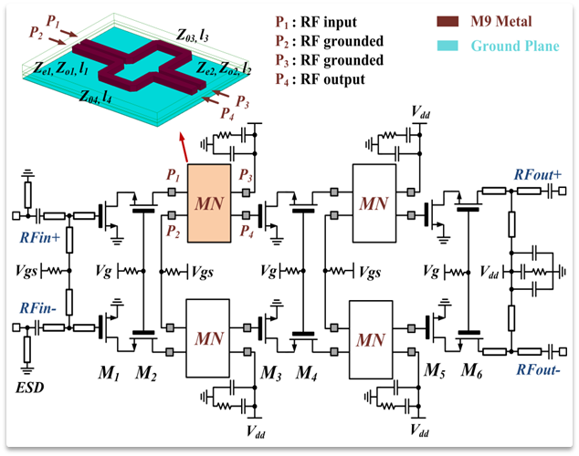
Fig.1 shows the Phase-locked Loop (PLL) architecture. Its consists of Phase frequency detector (PFD), Charge pump (CP), Loop filter (LF), Voltage-controlled oscillator (VCO) and Feedback divider (FBD) and Serial-to-parallel interface (SPI). The DSM is essential block if a fractional function is required. Fig. 4. gives the schematic of the VCO. Its frequency is tuned by employing accumulation-mode MOS varactors. The VCO frequency can be approximated as
where L, Cvar, and Cp respectively represent the inductance, varactor capacitance, and loading capacitance at the resonator. For VCO operates such at 40 GHz, the Q factor of the varactor and capacitor are the critical parameters. On the other hand, the VCO should be covered more than 6 GHz frequency range for broadband applications. Also, to keep the gain Kvco in a reasonable value of the PLL system, a multi-band VCO employing capacitor bank is applied.
|
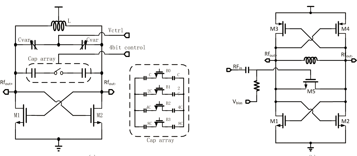 Fig. 2. Electrical schematic of the designed (a) VCO and (b) ILFD. Fig. 2. Electrical schematic of the designed (a) VCO and (b) ILFD.
|
The varactors (Cvar) is connected to the loop filter for analog voltage control. The capacitor bank consists of different value of capacitors with four switches ON and OFF with the help of a 4 bits digital control for frequency band control. The oscillation frequency bands overlap between them by careful capacitor size selection in the capacitor bank. The required 39GHz signal is generated and feeding to a buffer amplifier with differential output matching as shown in Fig. 2. All RF signals use microstrip transmission lines. After that the 18GHz output is done with the help of a Injection locked frequency divider (ILFD). This architecture has been chosen for its benefits lower power consumption and higher frequency capability. Conventional Source Couple Logic Divider (SCLD) are adopted for the frequency division after the ILFD in order to reduce the power consumption. The choice of the communication channel is done by a programmable divider implemented N-counter, that has a Division Factor Range (DFR) of 19 to 31. In order to obtain the wanted DFR, five bits are necessary to address the desired channels. Finally, the PFD, the CP and the 3rd order Loop Filter are implemented in order to detect the phase/frequency error and control the VCO with the analog control voltage. The overview of the designed PLL is located in the middle of the fabricated transceiver RFIC.
|
 |
 |
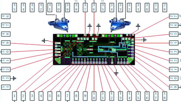
| Layout and bond wire diagram of the PLL |
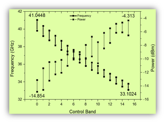
Measured frequency and amplitude against the control bit |
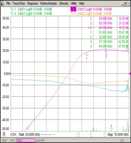
Measured results
- Voltage: 1V
- Current: 32mA (without buffer)
- Frequency: 33.1~41GHz
- Phase Noise: -92~-102 dBc/Hz @ 1 MHz offset
|
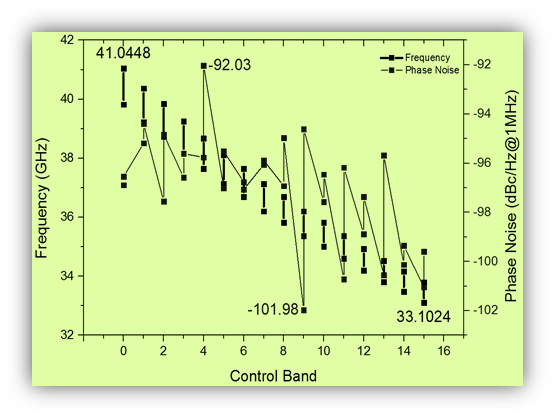 |
| Measured frequency and phase noise against the control bit |