60 GHz RFIC Transceiver for Short Range Instant Massive Data Sharing
The project is funded by HKSAR Innovation and Technology Commission
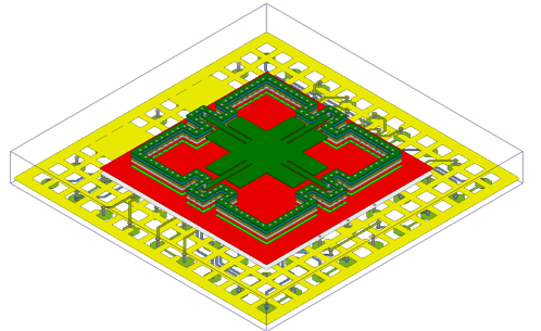
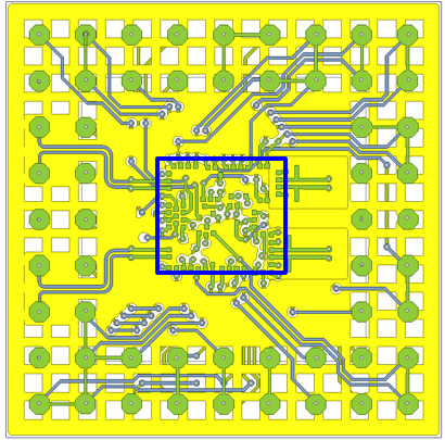
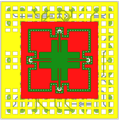
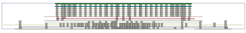
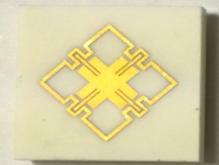
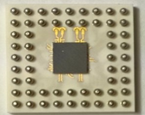
PackagingThe design of the package mainly focuses on antenna and interconnection design (flip chip bonding, through via transition modeling and feeding network). In this project, the packaged transceiver module is realized on 12-layer LTCC substrate. The thickness of the module is about 1.3 mm including an embedded antenna and its feed network. Interconnections between the antenna and RFIC utilize 50 transmission lines. The input and output IF signals and all the bias connections are routed to the PCB using Ball Grid Array (BGA) connections on the bottom side of the LTCC as shown in Fig 4.a. In this work, flip chip process is based on Au stud bumps. The diameter of the bumps is about 60 um. The final step in the assembly process is the BGA soldering, then the module was reflow-soldered onto a PCB. Photographs of the complete LTCC module is depicted in Fig 4.b.
| |||||||||||||||