ITF project
A collaboration of
City University of Hong Kong
C & L Holdings Ltd
and Elec & Eltek Multilayer PCB Ltd
The project is supported by Innovation and Technology Fund (ITF), HKSAR [Project No. ITS/049/11FP].
Home | | Contact Us
Projects
Unique features
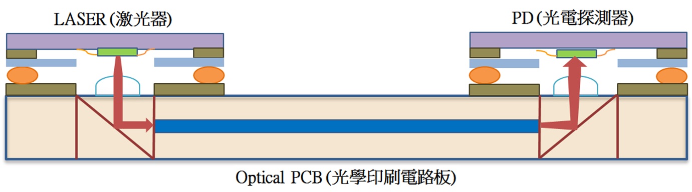
- Standard Lithography and PCB technology processing
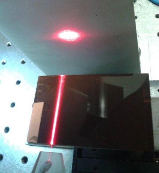
- Optical Fiber or Waveguide as the transmission channel
- High transmittance @ 850 nm
- High heat and pressure resistance
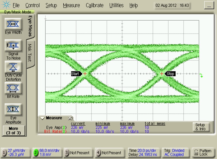
- 12 Channels for 10Gb/s, total 120Gb/s
Technical data
| Substrate Standard | FR4 (5x5 inch) |
| Lamination | Standard temperature > 180 °C, pressure 23 kp/sq. cm |
| Standard tests Reflow | 3 times for 10 s solder floating at 260 °C |
| Optical loss |
|
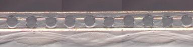
Fiber PCB Cross Section
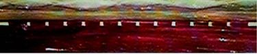
Waveguide PCB Cross Section
10Gb/s Eye Diagram
Fibre PCB Top View

Waveguide PCB Top View
Update
Video on fiber-embedded PCBs
Demonstration of 10G fiber-embedded PCB prototypes of a size not less than 5" x 5"using standard 50/125 microns multimode glass fibers
Click to watch ...
Video on waveguide-embedded PCBs
Demonstration of 10G waveguide-embedded PCB prototypes of a size not less than 5" x 5", where the polymer waveguides have a cross-sectional size of 50 x 50 microns.
Click to watch ...