60 GHz RFIC Transceiver for Short Range Instant Massive Data Sharing
The project is funded by HKSAR Innovation and Technology Commission
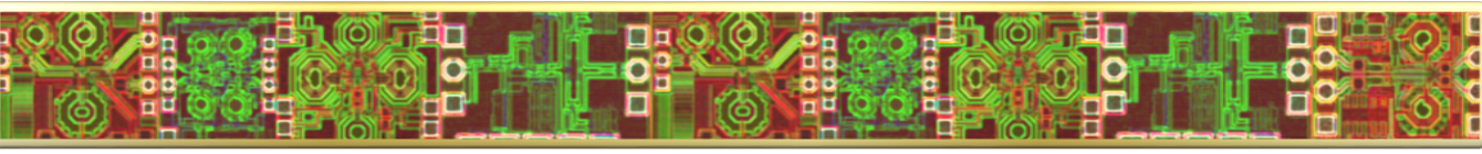
RFIC DesignSilcon-Based Transceiver ModuleFig. 2. Die micrograph of the 3.1x3.1 mm2 60GHz transceiver RFIC.
60 GHz double-conversion TX and RX architectureFig.2 gives the die micrograph of the transceiver. It is separated into three part, TX is located at upper area and PLL is located in middle are while the RX is located in bottom area. The RX consists of the LNA, 40GHz down conversion mixer, VGA and 20GHz down conversion mixer. The LNA is a three stages differential common-source common-gate(CS-CG) amplifier with 22 dB gain and about 20 GHz bandwidth. Moreover, in order to obtain better noise performance, the matching networks of the first stage are chosen for noise matching, while the inter-stages are conjugate matched to complex impedances for higher power gain. All the matching networks and interconnections are implemented using the thin-film microstrip transmission lines. All lines are kept as short as possible to minimize loss and the circuit size. The VGA is designed to have a conversion gain of 30 dB with gain control range output by the external control. The 36 GHz output of the PLL drives the 1st down conversion mixer and then this 36GHz signal is divided by 2 to 18 GHz LO signal to drive 2nd down conversion mixer. Both mixers are designed in double balanced configuration and the image rejection of the four channels at 3.6GHz IF are around 25-32 dB. The differential baseband output are fed to the external saw filter thought the bond wire. The complete receiver analogue frontend has about 41 dB conversion gain and the power consumption is 191 mW. The TX exhibits the similar architecture of the RX. A differential architecture is adapted from antenna to baseband because of its common-mode rejection ability. The saturated output power of the power amplifier is around 5 dBm delivered to differential antennas. |