Single-crystal lithium niobate (LiNbO3, LN) is an excellent nonlinear optical material that is widely used
in telecommunications and nonlinear optics. Conventional LN components, however are realized in weakly-perturbed LN waveguides
with very low index contrast (Δn ~ 0.02) and large device dimensions. An integrated LN nanophotonic platform, which combines the
unique material properties of LN with the superior light confinement in wavelength scale optical waveguides and cavities, could
overcome these limitations and enable efficient, low-cost and highly-integrated nonlinear optical systems.
Based on thin-film LN substrates and standard nanofabrication approaches, we have developed nanophotonic LN devices with ultra-high
quality factor (~ 10,000,000) and extremely low propagation loss of 3 dB/m
[Optica 4(2017)].
The high-confinement and low-loss lithium niobate photonic circuit could enable a range of electro-optic and nonlinear-optic applications
ranging from telecommunications to quantum information processing. Check out
Harvard Press Release
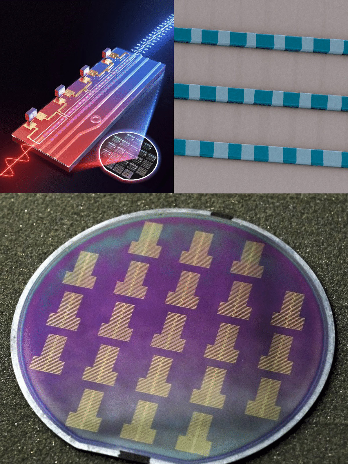
Our recent research efforts focus on further scaling up these low-loss elements into LN photonic integrated circuits (PIC) with wafer-scale
manufacturability and advanced functionalities. We demonstrate 4-inch wafer-scale fabrication of thin-film LN PICs using an i-line (365nm)
optical stepper lithography system (NFF, HKUST) and Ar+-based reactive ion etching (CityU). Thousands of high-performance devices, either
standalone or cascaded, could be realized in one shot, with measured optical loss below 0.15 dB/cm and intrinsic Q factors beyond 6 million.
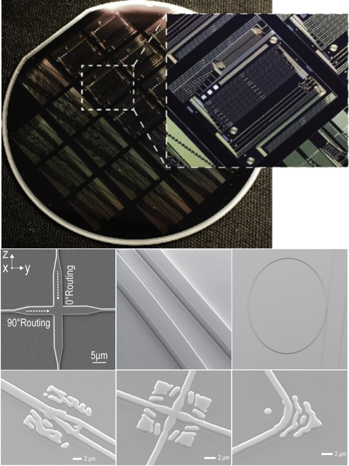
What’s more, we also introduced the gradient-based inverse design method tailored for LNOI platform which considered all fabrication constraints
including minimum feature size and sidewall angle. Building blocks with low loss and compact footprints were achieved.
High-performance electro-optic modulators plays a crucial role in converting electrical signals into the optical domain at high speeds, making them
essential components for optical fiber communications, microwave photonics and various optoelectronic applications. However, traditional LN modulators,
which have been widely used for many decades, are typically realized in discrete (non-integrated) form due to the lack of appropriate nanofabrication techniques.
This limitation has resulted in significant trade-offs in key modulator metrics. One particular challenge with traditional LN modulators is their inability to
directly utilize electrical signals from CMOS circuits due to their high driving voltage (> 3.5 V). This means that special electrical amplifiers are needed,
which can be both expensive and power consuming.
To overcome these limitations, our lab utilized the low-loss and high-confinement properties of our LN nanophotonic platform to develop integrated LN modulators
with exceptional performance. By harnessing the excellent material properties of LN and utilizing microfabrication techniques for integration, we can create chip-scale
LN modulators that are significantly smaller in size, consume orders of magnitude less power, and enable data transmission at much higher rates. These ultra-high-performance
LN modulators hold great potential for future optical fiber networks, particularly in long-distance and data center communications. They offer advantages such as improved efficiency,
reduced cost, and enhanced data transmission capabilities. See more in our paper featured in
Nature.
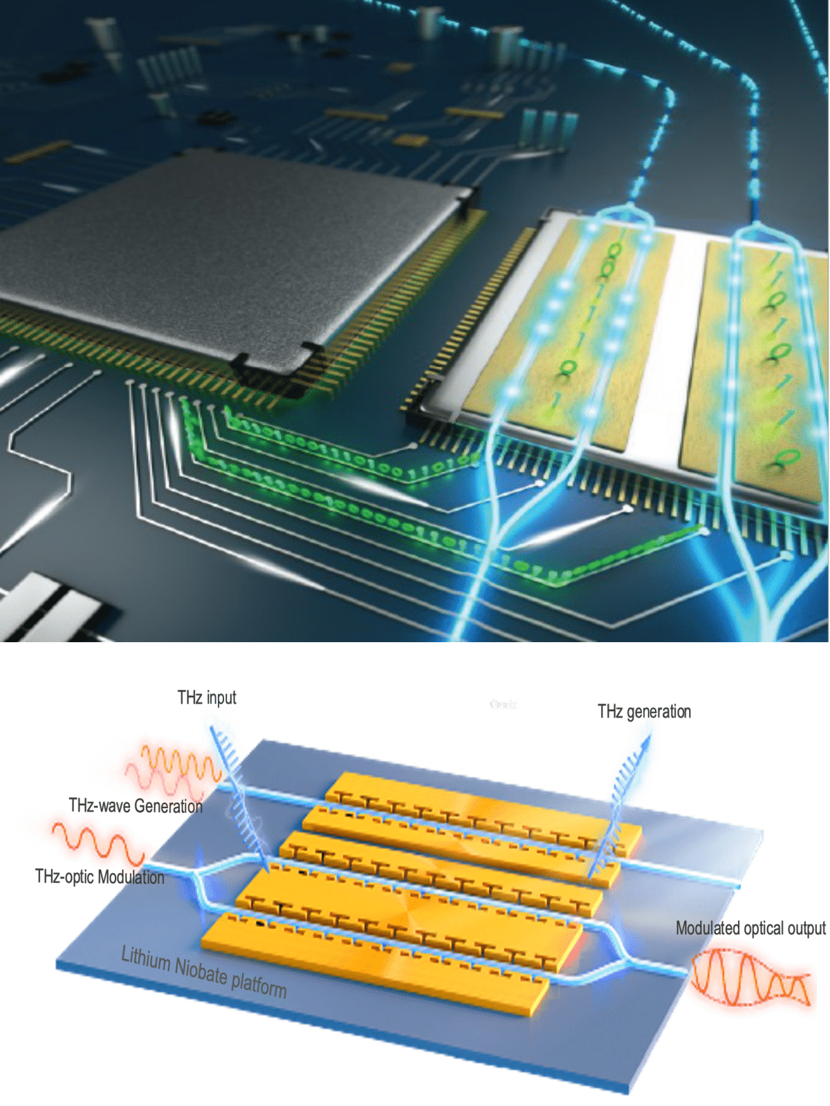
More recently, we have further leveraged the testing capabilities at the State Key Laboratory of Terahertz and Millimeter Waves, CityU to push the operation bandwidths of LN modulators
deep into the millimeter-wave (mmWave) and terahertz (THz) frequency ranges, reaching up to 500 GHz. By fabricating mmWave-optic modulators on silicon substrate and THz-optic modulators
on quartz substrate, we can efficiently convert mmWave/THz signals into the optical domain. These modulators have the potential to become crucial components for long-haul transmission and
processing of 6G wireless signals through optical networks. We employ precise electrical measurements to characterize and model the transmission line loss as well as the velocity- and
impedance-matching conditions at these ultrahigh frequencies. Based on our experimentally verified model, we have successfully demonstrated thin-film lithium niobate mmWave-optic modulators
with a measured 3-dB electro-optic bandwidth of 170 GHz and a 6-dB bandwidth of 295 GHz. Further details can be found in our paper published in Photonic Research. Most recently, we have further
pushed the modulation bandwidth into the THz regime (up to 500 GHz), achieving a half-wave voltage of 6 V at 300 GHz and 8 V at 500 GHz. This breakthrough has significantly implications for THz
communications, remote sensing, and the broader field of THz photonics.
Microwave photonics (MWP) is a powerful technology that makes use of optical devices and systems to perform microwave signal generation, manipulation and transmission tasks.
Recent advances in photonic integration have propelled microwave photonic technologies to new heights, allowing a dramatic reduction in the footprint, weight and power consumption of MWP systems.
Integrated LN photonics is a particularly attractive platform for future chip-scale MWP systems owing to its unique electro-optic properties, low optical loss and excellent scalability, offering
the promise of integrating active and passive MWP components all in one chip.
A key enabler for such systems is a highly linear electro-optic modulator that could faithfully covert analog electrical signals into optical signals. In our lab, we take advantage of our low-loss
LN nanophotonic platform to develop ultra-high linearity integrated LN modulators, by combining the intrinsically linear electro-optic response of LN and an optimized linearization strategy
(ring-assisted MZI configuration). We demonstrate modulators with ultra-high spurious-free dynamic range (SFDR) of 120.04 dB·Hz4/5 at 1 GHz. See more details in our paper featured in
Photonics Research.
More recently, we further combine the high-performance EO modulation block and a multi-purpose low-loss signal processing section on the same LN chip to demonstrate an ultrafast MWP signal processing engine,
which can perform multi-purpose processing and computation tasks of analog signals up to 256 giga samples per second (GSa/s) at CMOS-compatible voltages. Such MWP engine exhibits significant and all-around
performance edges in terms of operation bandwidth, processing speed and energy consumption compared with other on-chip and off-chip MWP platforms, and could find a variety applications in future wireless
communications, Internet of things, high-resolution radar systems and photonic artificial intelligence.. See more details in our paper featured in
Nature.
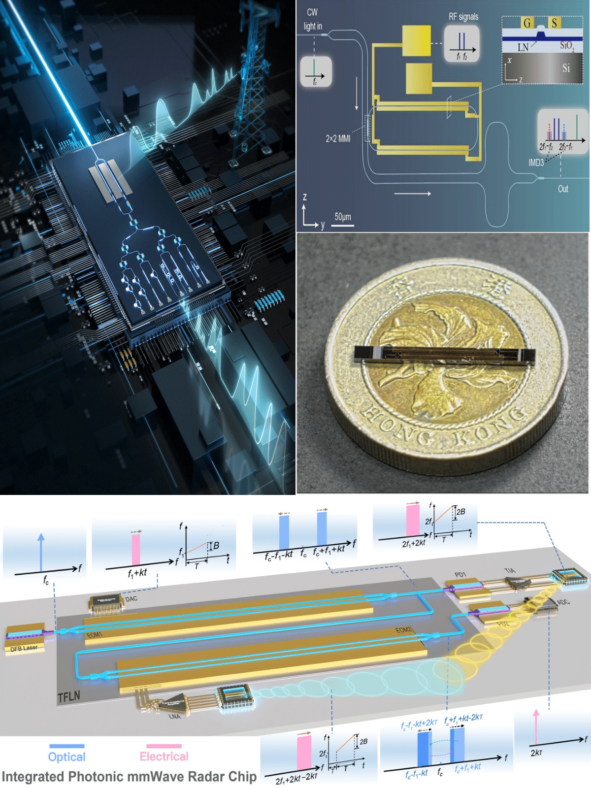
Our chip-scale MWP platform has also enabled the first integrated photonic radar that operates in the mmWave band (40-50 GHz) based on a 4-inch wafer-scale thin-film lithium niobate (TFLN) technology, achieving
multi-target ranging and inverse synthetic aperture radar imaging with centimeter-resolution. Our integrated TFLN photonic mmWave radar chip provides a compact and cost-effective solution in the 6G era for high-resolution
sensing and detection in vehicle radar, airborne radar, and smart homes. See more details in our paper feature in
arXiv.
Optical frequency combs, with equally spaced spectral lines in the frequency domain, are excellent broadband coherent light sources and precise
spectral rulers that have wide applications in optical clocks, pulse shaping, spectroscopy, telecommunications, light detection and ranging (LiDAR),
and quantum information processing. In recent years, chip-scale frequency comb generation, mostly based on χ(3) has emerged as a particularly
promising candidate for the miniaturization of comb systems.
Remarkably, LN’s strong χ(2)/Pockels effects can also be used to directly generate frequency combs. Compared with Kerr combs, electro-optic (EO)
combs can be generated at arbitrary optical powers (threshold-less), can be flexibly controlled using microwaves, and usually have good noise properties due
to the low-noise nature of microwave sources. It is well known that EO frequency combs can be generated by passing a continuous-wave laser through a phase modulator.
However, such devices usually generate only tens of lines and span only a few nanometers since the light only passes the modulation area once. By embedding the electro-optic
frequency comb generation process into a high-Q LN microcavity, the light can circulate in the resonant cavity and pass through the modulation area multiple times, resulting
in much broader frequency combs (> 90 nm). See more details in our paper featured in
Nature.
The resonant EO combs discussed above are typically limited by the equally spaced resonances in a whispering-gallery modes resonator, leading to a fixed roll-off comb spectral shape.
Recently, we have successfully demonstrated the arbitrary spectral shaping of resonant EO combs by introducing a frequency “boundary” using a photonic-crystal ring resonator.
Our gradient photonic crystal ring design enables a controllable and reliable generation of single frequency splitting on an anisotropic x-cut LN platform. The precise control of EO comb
spectral shape is of critical importance to both the exploration of fundamental high-dimensional physics and practical nonlinear optics applications. See more details in our paper featured as inside front cover in
Advanced Materials.
On the other hand, compared with resonant schemes, non-resonant EO comb generation offers better flexibility in selecting and tuning the repetition rate and operation wavelength on demand. However, it usually requires
large RF drive power and features relatively narrow comb span. We address this issue using a multi-loop design where light passes through the modulation electrodes for 4 round trips with the assistance of multiple mode
conversion processes, leading to a measured 15 times reduction in modulation power consumption. See more details in our paper featured in
Communications Physics.
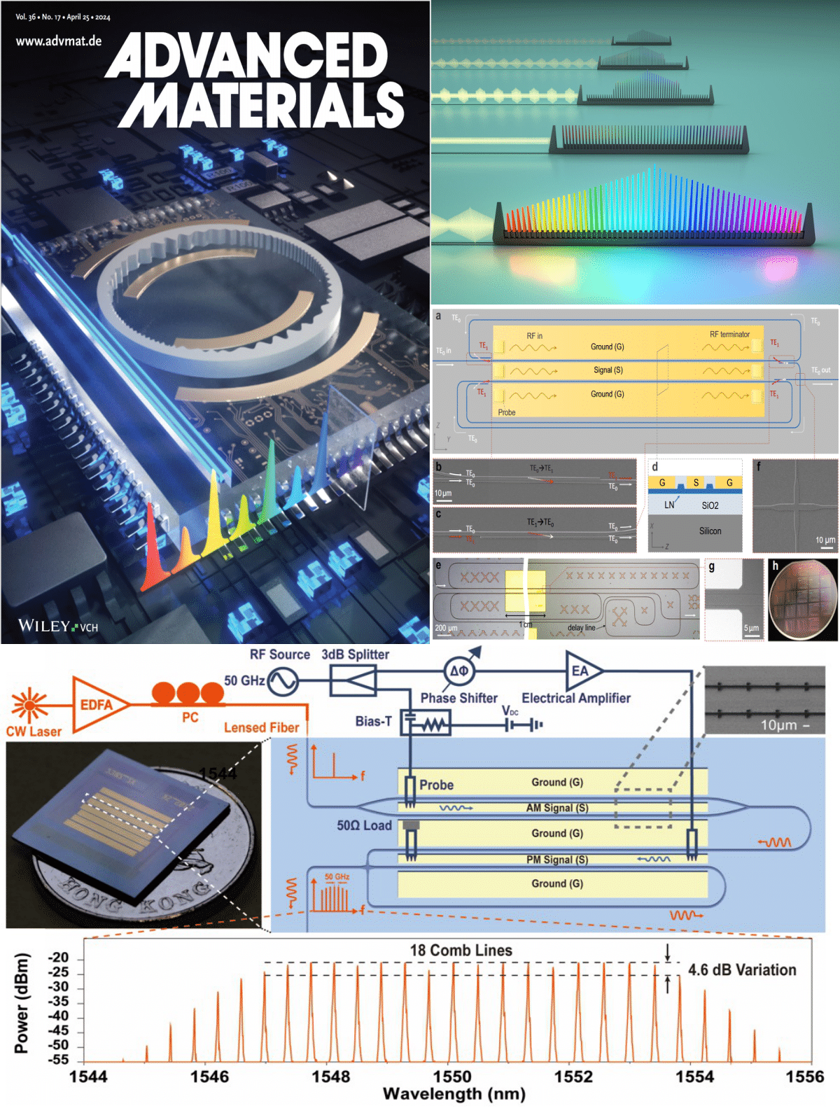
We further make use of the non-resonant scheme to demonstrate
a flat-top EO comb through cascaded amplitude and phase modulators on-chip with 50 GHz comb line spacing, power variation < 4.6 dB over 18 channels, which enables a wavelength-division multiplexing (WDM) transmission with a
total bit rate of 6.48 Tb/s over a 53-km field-deployed link across Hong Kong. See more details in our conference paper at OFC 2024.
Second order (χ(2)) nonlinear optical processes, including second harmonic generation (SHG), sum/difference frequency generation (SFG/DFG),
and spontaneous parametric down conversion (SPDC), not only are crucial for accessing new spectral ranges in classical optics, but also act
as key resources for non-classical light generation in quantum information processing. In this project, we utilize our thin-film LN nano
waveguides to design devices that can efficiently convert the color of light from near-infrared to visible. The strong light confinement
in our waveguides can boost the efficiency of this process by orders of magnitude compared with conventional weakly-confined devices.
The top-down fabrication method we use also allows us to precisely engineer the dispersion properties and phase-matching conditions.
See more in our paper featured in
Optica.
Recently, we have further pushed the PPLN fabrication processes toward wafer scales. However, thickness variation issues will appear and compromise
the performance of our devices in wafer-scale systems. To overcome this, we have utilized a segmented heater design to counteract the phase mismatching
issue induced by wafer-thickness variation, leading to a notable normalized conversion efficiency of nearly 3800%W-1cm-2. This opens the door to a wide
range of applications such as optical parametric amplification (OPA) in data communication and squeezed light generation in quantum optics.
For more comprehensive information, see our recently posted paper on
arXiv.