Single-crystal lithium niobate (LiNbO3, LN) is an excellent nonlinear optical material that is widely used
in telecommunications and nonlinear optics. Conventional LN components, however are realized in weakly-perturbed LN waveguides
with very low index contrast (Δn ~ 0.02) and large device dimensions. An integrated LN nanophotonic platform, which combines the
unique material properties of LN with the superior light confinement in wavelength scale optical waveguides and cavities, could
overcome these limitations and enable efficient, low-cost and highly-integrated nonlinear optical systems.
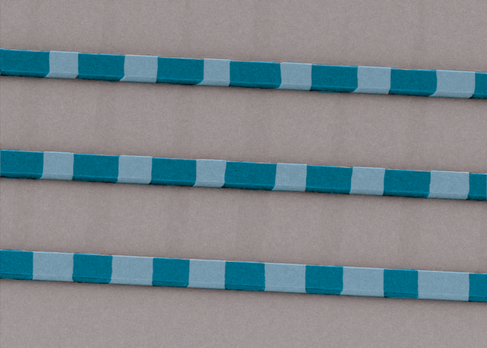
Based on thin-film LN substrates and standard nanofabrication approaches, we have developed nanophotonic LN devices with ultra-high
quality factor (~ 10,000,000) and extremely low propagation loss of 3 dB/m
[Optica 4(2017)].
The high-confinement and low-loss lithium niobate photonic circuit could enable a range of electro-optic and nonlinear-optic applications
ranging from telecommunications to quantum information processing. Check out
Harvard Press Release
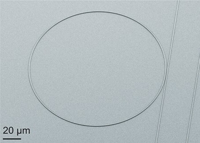
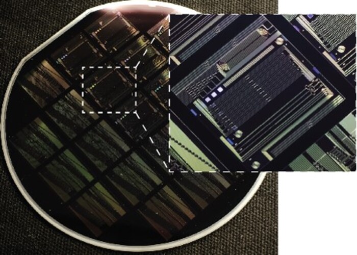
Our recent research efforts focus on further scaling up these low-loss elements into LN photonic integrated circuits (PIC) with wafer-scale
manufacturability and advanced functionalities. We demonstrate 4-inch wafer-scale fabrication of thin-film LN PICs using an i-line (365nm)
optical stepper lithography system (NFF, HKUST) and Ar+-based reactive ion etching (CityU). Thousands of high-performance devices, either
standalone or cascaded, could be realized in one shot, with measured optical loss below 0.15 dB/cm and intrinsic Q factors beyond 2 million.
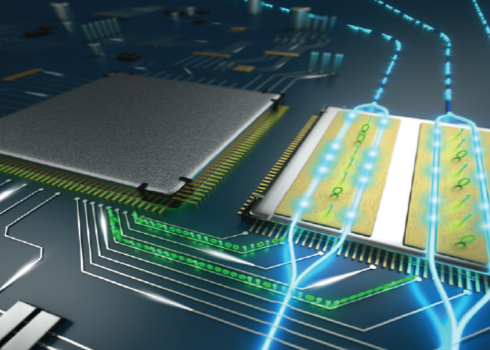
High-performance electro-optic modulators that convert electrical signals into optical domain at high speeds, are key
components for optical fiber communications and many other optoelectronic applications. Traditional LN modulators, as the most widely
used platform for decades, however have remained in their discrete form due to the lack of appropriate nanofabrication techniques,
resulting in significant trade-offs in key modulator metrics. In particular, these modulators cannot directly use the electrical signals
from CMOS circuits because of their high driving voltage (> 3.5 V). They require special electrical amplifiers that are prohibitively
expensive and power-consuming for next-generation fiber networks.
In our lab, we take advantage of our low-loss and high-confinement LN nanophotonic platform to develop ultra-high performance integrated LN
modulators. By combining the superior material properties of LN and microfabrication-enabled integrability, we can realize chip-scale LN
modulators that are dramatically smaller, cost orders of magnitude less power, and transmit data at much higher rates. Such systems are
ideal for future optical fiber networks for long-distance and data center communications. See more in our paper featured in
Nature.
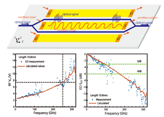
More recently, we have further leveraged the testing capabilities at the State Key Laboratory of Terahertz and Millimeter Waves,
CityU to push the operation bandwidths of LN modulators deep into the millimeter-wave (mmWave) bands (up to 300 GHz). mmWave-optic
modulators that could efficiently convert mmWave signals into optical domain could become crucial components for long-haul transmission
of mmWave signals through optical networks. We use precise electrical measurements to characterize and model the transmission line loss
as well as the velocity- and impedance-matching conditions at these ultrahigh frequencies. Based on our experimentally verified model,
we demonstrate thin-film lithium niobate mmWave-optic modulators with a measured 3-dB electro-optic bandwidth of 170 GHz and a 6-dB bandwidth
of 295 GHz. The device also shows a low RF half-wave voltage of 7.3 V measured at an ultrahigh modulation frequency of 250 GHz. See more
in our paper recently posted on
arXiv.
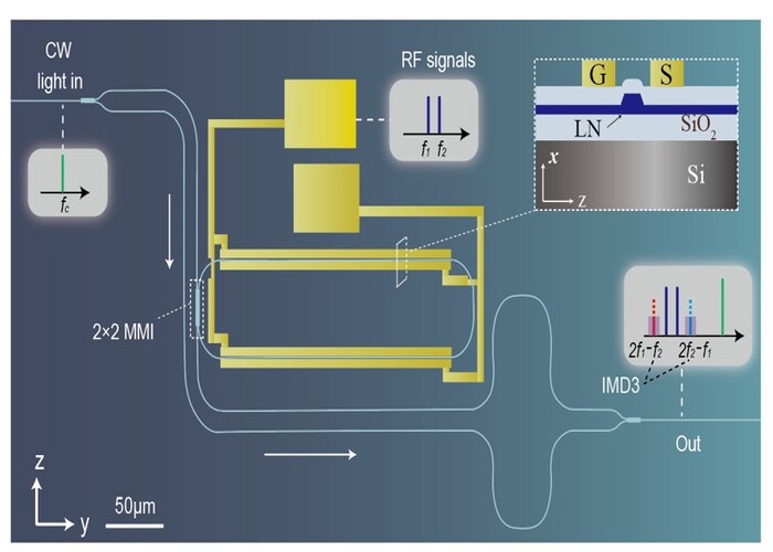
Microwave photonics (MWP) is a powerful technology that makes use of optical devices and systems to perform microwave signal generation,
manipulation and transmission tasks. Recent advances in photonic integration have propelled microwave photonic technologies to new heights,
allowing a dramatic reduction in the footprint, weight and power consumption of MWP systems. Integrated lithium niobate (LN) photonics is a
particularly attractive platform for future chip-scale microwave photonics systems owing to its unique electro-optic properties, low optical
loss and excellent scalability, offering the promise of integrating active and passive MWP components all in one chip.
A key enabler for such systems is a highly linear electro-optic modulator that could faithfully covert analog electrical signals into optical
signals. In our lab, we take advantage of our low-loss LN nanophotonic platform to develop ultra-high linearity integrated LN modulators, by
combining the intrinsically linear electro-optic response of LN and an optimized linearization strategy (ring-assisted MZI configuration).
We demonstrate modulators with ultra-high spurious-free dynamic range (SFDR) of 120.04 dB·Hz4/5¬ at 1 GHz. Further integration of these linearized
modulators with frequency comb sources, tunable filters, programmable switches and low-loss delay lines could lead to chip-scale MWP systems with
unique functionalities that are not currently achievable in other photonic platforms, enabling advanced MWP applications like broadband RF signal
generation, radio-over-fiber links and RF-photonic signal processing. See more in our paper recently posted on
arXiv.
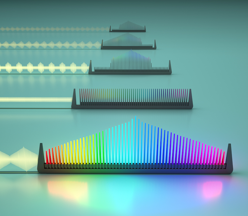
Optical frequency combs, with equally spaced spectral lines in the frequency domain, are excellent broadband coherent light sources and precise
spectral rulers. In recent years, Kerr frequency comb generation based on high-Q microcavities has emerged as a particularly promising candidate
for a range of applications including optical clocks, pulse shaping, spectroscopy, telecommunications, light detection and ranging (LiDAR) and
quantum information processing. Although Kerr combs have been realized in various material platforms, realizing frequency combs in LN is still
of great interest to the comb community due to the existence of a strong χ(2) nonlinearity, which could be exploited to assist the
comb generation process and to achieve extra device functionalities.
Leveraging the high Q factors in our platform, we have demonstrated the generation of Kerr combs in dispersion-engineered LN microresonators.
More importantly, we can further combine LN combs with its χ(2) nonlinearity. For example, by cascading a second microring resonator
as a tunable filter, the generated Kerr comb spectrum can be further shaped and manipulated on the same chip. See more details in our paper
featured in Nature Communications.
Remarkably, without the need for χ(3) nonlinearity, LN’s strong χ(2) effects can also be used to directly generate a
broadband frequency comb in LN microcavities. It is well known that electro-optic frequency combs can be generated by passing a continuous-wave
laser through a sequence of phase and amplitude modulators. However, such devices usually generate only tens of lines and spanning only a few
nanometers. By embedding the electro-optic frequency comb generation process into a high-Q LN microcavity, such process can be dramatically
enhanced, resulting in much broader frequency combs (> 90 nm). Compared with Kerr combs, electro-optic combs can be generated at arbitrary
optical powers (threshold-less), can be flexibly controlled using microwaves, and usually have good noise properties due to the low-noise nature
of microwave sources. See more details in our paper featured in
Nature.
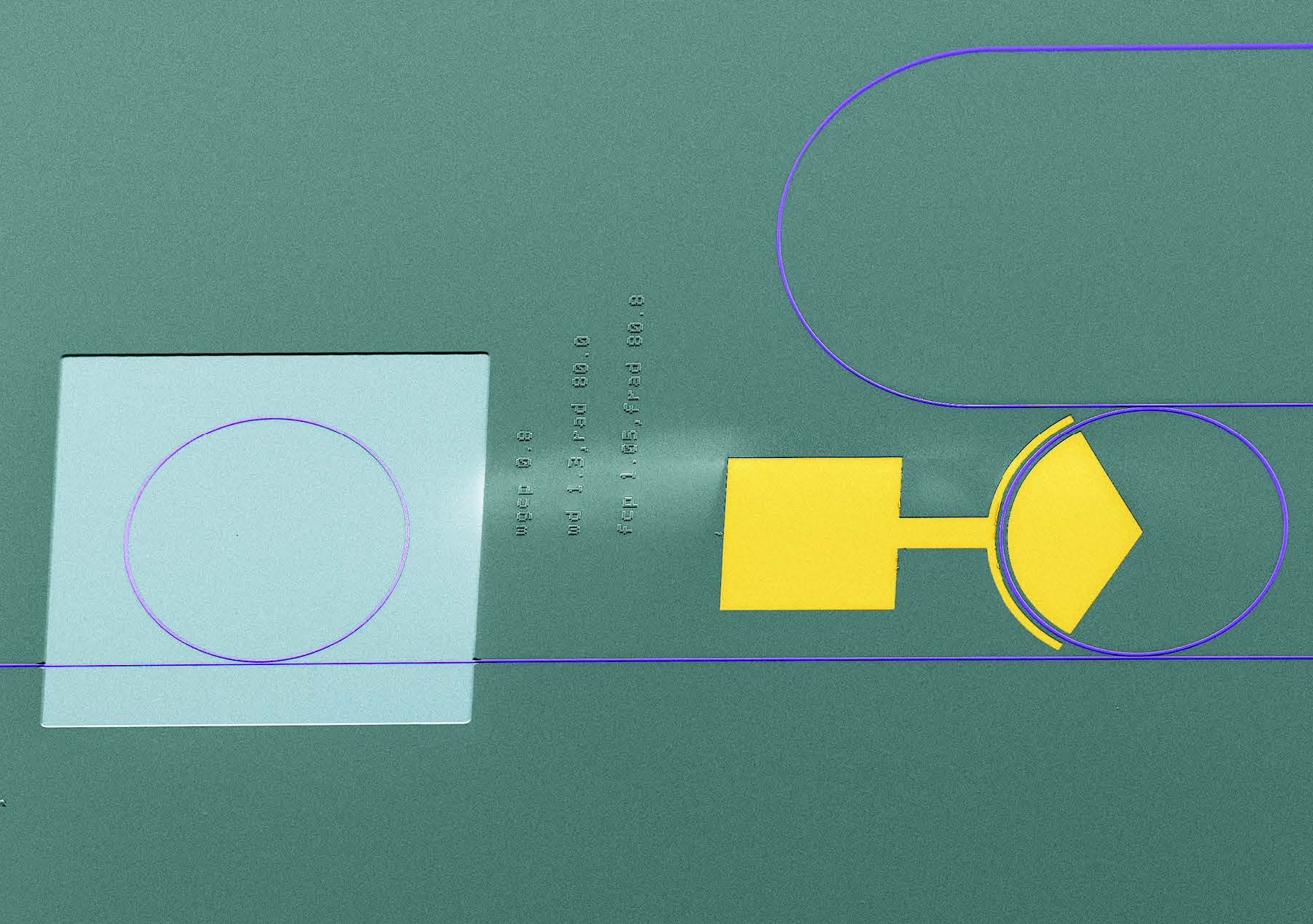
Second order (χ(2)) nonlinear optical processes, including second harmonic generation (SHG), sum/difference frequency generation (SFG/DFG), and parametric down conversion, not only are crucial for accessing new spectral ranges in classical optics, but also act as key resources for non-classical light generation in quantum information processing. In this project, we utilize our thin-film LN nanowaveguides to design devices that can efficiently convert the color of light from near-infrared to visible. The strong light confinement in our waveguides can boost the efficiency of this process by orders of magnitude compared with conventional weakly-confined devices. The top-down fabrication method we use also allows us to precisely engineer the dispersion properties and phase-matching conditions. Such devices are promising for on-chip quantum wavelength conversion at the single-photon level. See more in our paper featured in Optica.